LARGE AREA MASTERING


INTERFERENCE LASER LITHOGRAPHY

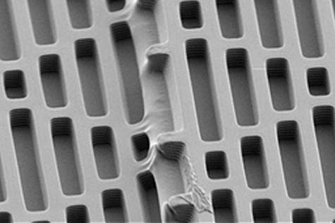
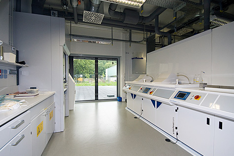
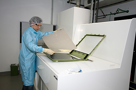
Interference lithography is an unique technology to fabricate highly periodic as well as stochastic surface relief structures in photoresist materials. By modification of process parameters, a large variety of different profile shapes can be generated. One- and two-dimensional structures are realized, whereas the structure geometry could be sinusoidal, parabolic, triangular or even binary. The strength of interference lithography is its upscaling potential to very large, seamless structured areas with a beautiful homogeneity (up to one square meter and even larger). After generating photoresist masters, copying processes by common replication technologies allow the highly cost-effective production of large area fi lm products as well as small structured polymer products.
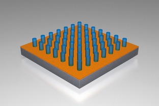
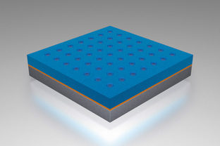
图示干涉式蚀刻法

干涉式激光蚀刻
特大面积母板

图示干涉式蚀刻法

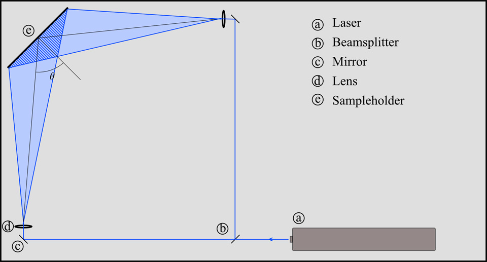
The interference etching method is using the mirrors and the lens to bifurcate a specified wavelength beam, then widen them and cross them to form into a sinusoidal interference to do the exposure of the resist. The pattern thus exposed is of a consistent specification on a flat plane. Its cycle is decided by the angle of incidence. Nowadays, the 351nm wavelength is more commonly used. The spacing of the pattern can be less than 200nm. If more narrow is required, the resist and the light beam must be more matching.

NANOIMPRINT

Nanoimprint lithography is a method of fabricating nanometer scale patterns. It is a simple nanolithography process with low cost, high throughput and high resolution. It creates patterns by mechanical deformation of imprint resist and subsequent processes. The imprint resist is typically a monomer or polymerformulation that is cured by heat or UV light during the imprinting. Adhesion between the resist and the template is controlled to allow proper release.
图示

步进重复式的纳米压印法
边缝位

RTR NANOIMPRINT

Roll to roll (RTR) nanoimprint is the ideal production tool. It can imprint directly onto the thin film or the UV resist. But the simplicity of the imprint process does not mean that the machine is simple. For example, the cylinder shape imprint mold is a challenge. For imprint onto the thin film, we will make a thin nickel mold and lay it onto a metal cylinder. If the imprint target is the UV resist, we will accordingly make a soft transparent thin mold and lay it onto a transparent cylinder. Nowadays, if the imprint pattern is the 100nm range, the RTR speed can be 5 meters per minute.
软模
膜模片
UV LITHOGRAPHY


UV LITHOGRAPHY

We use UV lithography as a key mastering process for microstructures down to 1 μm feature size. UV-lithogaphy is well known in the semiconductor technology for wafer sizes (4-12 inch). Over several years temicon has consequently devoloped UV lithography and now has technological USPs in terms of e.g. large formats (square meter), high aspect ratios (above 2,0), precisely adjustable sidewall angles or gapless lens arrays. In this manner, a large variety of microstructures with customized functionalities can be realized.

Two UV lithography lines for

• wafer formats (up to 200 mm)
• large formats (up to 800 x 1200 mm)

are in operation in our 400 sqm cleanroom facility, including resist coating, exposure, wet processing and sputtering.
图示

旋涂 500mm x 600mm 玻璃基板
大面积 UV 曝光
ELECTROFORMING


ELECTROFORMING

Electroforming can be used to produce a metallic copy of patterned photoresist masters, thus transforming sensitive micro/nanostructures made of photoresist into a robust metal tool.

For this purpose, a thin metal layer is sputtered on the patterned resist surface. Afterwards, a nickel shim is deposited by electroforming. Typical thicknesses of the shims are in the range of 50 μm up to a few millimeter. The shim is finally laser or wire cut exactly to the required dimensions and if necessary laser welded to a sleeve. temicon is working on the development of next generation sleeves. These sleeves will be seamless, offering highest efficiency and new fields of application for patterned films. In a similar way, metal parts are electroformed. In this case the galvanic deposition is stopped right before reaching the top of the resist pattern, thus achieving the micro-hole structures in the metal parts.
电铸硅板设置
电铸板
电铸程序 UV-Li Ga 代替光蚀剜或激光切割