NANOIMPRINT TOOLS


CNI- UV & 热压纳米压印

CNI V2.0 - Desktop Nanoimprint Tool


Nanoimprint has never been more simple…


Featuring:
• Thermal nanoimprint (temperature up to 200ºC)
• UV nanoimprint (wavelength 365 nm)
• Imprint in vacuum (0.1 mbar)
• Plug and play

The CNI v2.0 is a very flexible nanoimprint tool. It offers thermal and UV nanoimprint and imprinting in vacuum if needed. The system is build from modules that makes it very flexible to configure for specific needs and to store away when not in use. It handles all shapes and formats of stamps and substrates up to Ø100 mm (4-inch). The system has manual loading and unloading of stamp and substrate but all processing are fully automatic and the dedicated software gives the user full control of the imprint process.

CNI v2.0 one-page flyer (PDF)

EZI-UV NIL

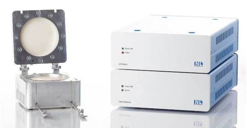
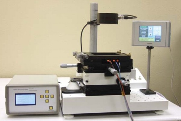
EZI NANOIMPRINT SYSTEM AR- NTP-400/600

EZImprinting (EZI) is a revolutionary super-high yield (> 99 %) nanoimprint lithography platform with sub-10nm resolution and one-step Auto Release™ function. EZI provides a bench-top, stand-alone nanoimprint platform: the AR-NTP-400/600.


Featuring:
• Full-wafer imprinting - 4 inch (NTP-400) or 6 inch (NTP-600)
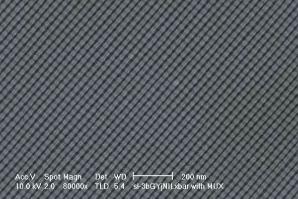
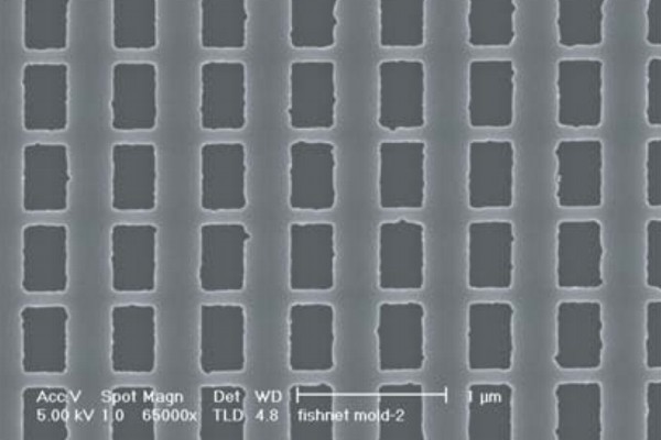
• Sub-10 nm resolution with 99% yield - the highest in the world!
• One step auto-release function preventing mold/substrate damage
• Supports both hard and soft molds
• Variable mold and substrate sizes
• Programmable PLC with touch-screen user interface
TECHNOLOGY


LED

There are several ways to improve light outcoupling efficiency of LEDs by the use of nanostructures. With nanoimprint, one approach is to place the nanostructures on top of the LEDs while another way is to make the LEDs on patterned sapphire substrates (PSS), where nanoimprint is used for cost efficient fabrication of the PSS.

NILT works with several LED companies and has great experience in making wafer sized NIL stamps or molds with sub-wavelenght dot patterns or photonic bandgap structures (PBG), used directly in a NIL process for patterning of LEDs or used as masters for making polymer NIL stamps.

MICRO FLUIDICS

A great advantages of hot embossing is its capability to directly pattern polymers with micro and nanostructures. This is advantageous for applications where polymer is used as part of the final product. It can be exploited by creating µm and nm sized fluidic networks, even in different layers and in the same process step.

NILT supplies stamps or molds for hot embossing and/or nanoimprint lithography in silicon and nickel as well as transparent materials used with photo-curable polymers. NILT is building up injection molding competences and NILT also provides shims to be inserted into injection molding tools.